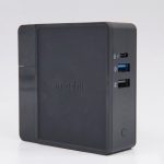
The Powerstation Hub by tech accessory maker Mophie is quite similar to the Anker PowerCore Fusion we reviewed earlier. It is a USB-C and USB-A wall charger that doubles as a portable battery, but also has the added benefit of featuring a Qi charging surface. And here's our teardown.
I Design

It is a black rounded square with a two-tone matte-and-glossy finish.

From top to bottom: USB-C bi-directional input and output port, two USB-A output ports, LED indicators, and power button.

The larger part of the case is covered with anti-slip silicon pads.

Input: 100V-240V,50/60Hz,0.25A. Input (USB-C PD): 5V2.4A, 9V2A, 12V1.5A. Total output: 18W. Qi wireless charging: 5W. Output: (USB-C PD): 5V2.4A, 9V2A, 12V1.5A. Output: (USB-A QC): 5V2.4A, 9V2A, 12V1.5A. Output: (USB-A): 5V2.4A. Battery: 3.6V, 6100mAh, 21.96Wh.

Interchangeable adaptor with foldable prongs.

It is also a power bank with 6100mAh capacity.

The thickness is 29.5mm/1.16inch.

It weights 259.7g/9.16oz.

Dimensions: 84 x 84 x 29.5mm. It is slightly bigger than the Apple 87W PD charger for MacBook Pro 15.

Press the power button and the LEDs light up.

It starts charging instantly when we put the phone on top.
II Teardown

Remove the adapter first.

Remove the glossy part of the casing.

Remove the larger cover.

Taking a look at the components.

Take the assembly out of the housing. We have a PCBA and two batteries.

Wireless charging coil and its PCBA on the other side.

The parts responsible for power management of the charger and power bank functions.

Next to the battery cell are components responsible for the power adapter part.

The transformer.

A UTC 7N65KL field effect MOS tube, primary switching tube.

A 400V, 22μF capacitor.

Input protection varistor.

A 0.22μF X capacitor.

A common mode choke.

Time delay fuse with letter code T2A for input protection.

A UTC, UPC817 feedback optocoupler.

A Y capacitor.

A 25V, 470μF capacitor.

White glue is filled between the components.

A 50V, 10μF capacitor powers the PWM controller.

Taking a look at the batteries.

18650 format, made by BAK with A31 letter code.

The battery is insulated with mylar tapes.

Two batteries are connected in parallel.

The parts responsible for power management of the charger and the power bank, with a daughter board connected to it with pins.

Remove the daughterboard.
An M-shaped foam isolation compartment around the LED indicator to prevent light leaks.

Close-up of the power button.

It has an LED indicator besides it.

Inductors and a few components on the back.

A Metal alloy inductor.

A 4R7 Metal alloy inductor.

101 filter inductor.

A boost IC with letter code 2330.

A Fitipower FP6730 step-up converter with letter code FC761K.

Detailed specifications of the Fitipower FP6730.

Let's take a look at the power management PCBA.

A magnetic loop inductor with heat shrink tube protection on the outside.

The Injoinic IP6528 is a buck converter with integrated synchronous switch, and an SoC that supports USB-C multi-protocol dual-port output. It supports dual port detection, single port fast charging output, dual port intelligent recognition 5V output, and can provide up to 45W output power. It also has line compensation function, as well as input overvoltage protection, undervoltage protection, output overcurrent protection, overvoltage protection, undervoltage protection, short circuit protection and other functions. It provides an all-rounded solution for applications including car chargers, power adapters, and smart sockets.

Detailed specifications of the Injoinic IP6528.

The controller chip for the power bank function also comes from Injoinic, model IP5328P. Thanks to its high integration with fewer components needed, the IP5328P is very suitable for PCB designs which require small footprint. The Injoinic IP5328P also integrates the QC2.0/QC2.0/QC 3.0 input/output fast charge protocol, and passed the QC3.0 Qualcomm certification with certificate number 4780056908-2. FCP, AFC, SFCP, MTK PE, USB C DRP, BC1.2 input/output charging protocols are all supported. It is worth mentioning that the IP5328P not only supports PD3.0/2.0 fast charging, but also PPS (Programmable Power Supply) at 5~12V.

Detailed specifications of the Injoinic IP6528P.

Eastsoft MCU, HR7P1698FGNF, for control functions.

A Zener tube.

An SS34A Schottky diode.

Xysemi XB8886A integrated protection tube for the battery pack.


A Zener tube.

A 2R2 Metal alloy inductor.

Solid capacitor 100μF, 16V.

Tiny components fill the back of the PCB.

There are three MLCC capacitors on the left.

SGM44599 toggle switch.

Two AONR21357 MOS tubes.

3PG small triode.

Taking a closer at the wireless charging part.

The wireless charging section is composed of a wireless charging coil, a magnetic isolation sheet, and a large PCBA on the back side.

The CPS EC8010 is a highly efficient, Qi-compliant, magnetic inductive wireless power transmitter IC for applications up to 5W. The system-on-chip integrates power controller, micro-controller, voltage regulator, foreign object detection (FOD), full bridge drivers and on-chip voltage and current demodulation. The EC8010 integrates one full bridge driver. Internal protection fuctions are provided for over current and over temperature. It has passed the CE/FCC/Qi-BPP certification.

Detailed specifications of the CPS EC8010.

DB207S patch rectifier bridge.

MPS MP6910A built-in MOS synchronous rectification IC.

On-bright OB2362 primary PWM controller.

The controller chip for power bank function is a Injoinic IP5306. The IP5306 is a multi-function power management SoC with integrated boost converter, lithium battery charge management, and battery level indication. It requires only one inductor for buck and boost functions. The synchronous boost system provides up to 2.4A of output current with conversion efficiency as high as 91%. It automatically enters sleep state when no load is present, and the quiescent current is reduced to 50uA. The chip requires fewer peripheral compnents, which can effectively reduce the size of the overall solution and reduce the BOM cost.

Detailed specifications of the Injoinic IP5306.

1R0 inductor.

Two MOSFETs from Vanguard Semiconductor, VS3640DS, dual MOS.

Detailed specifications of the VS3640DS.

MLCC capacitors.

All the components.
III Conclusion
The Mophie Powerstation Hub is a multiport charger, a power bank, and a Qi wireless charging pad all in one.
As a well-known brand that is featured in Apple store, the Mophie Powerstation Hub does not disappoint in our teardown. The neat design and layout, the use of high quality components, and thoughtful detail ensure the performance and longevity of the unit.
In terms of chip solutions, the wireless charging function is powered by CPS, and the power bank and charger function adopt Injoinic solution, all providing great performance with high efficiency.
However for the $99.95 asking price, an output power of 18W max is average, at best.
Pros:
Multiport charger/power bank/wireless charger all-in-one.
Thoughtful design and neat finish with high quality components.
Interchangeable adapter with foldable prongs.
Cons:
18W max output.
Expensive.
Source: chongdiantou

