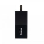
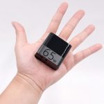
The Thinkplus PA65 65W PD charger by Lenovo is particularly popular among tech enthusiasts in China for its outstanding balance of power, size, and price (it has a nickname “the lipstick”). Measuring just 73 x 30 x 35mm / 2.9 x 1.2 x 1.4 inches (77cc), it is one of the most travel-friendly 65W chargers, despite the fact that there is no GaN inside. So how do the creators of this charger achieve this kind of excellence? There's only one way to find out.
I Unboxing

Our unit is a black Chinese domestic version. It has three color variants: black, red, and white.

Close-up of the package details.

A color-blocking red with specifications - a touch of Thinkpad.Model: PA65Input: 100V-240V~50/60Hz 1.5AOutput: 5V/3A, 9V/3A, 12V/3A, 15V/3A, 20V/3.25AIt is made by Powerland (a subsidiary of FSP, one of the world's largest power supply makers).

Opening the lid and tray box, our “lipstick” is laying in the tray.

Package contents: charger, user manual, and an E-marked 5A USB-C to USB-C cable with a cable tie.

The Thinkplus PA65 65W PD charger is a slender rectangular with rounded edges. It comes with a matte and glossy tow-tone finish and a tasteful “thinkplus” logo on the side.

The USB-C output port is in the center.

Specifications:Input: 100V-240V~50/60Hz 1.5AOutput: 5V/3A, 9V/3A, 12V/3A ,15V/3A, 20V/3.25A

Diemensions: 73 x 30 x 35mm / 2.9 x 1.2 x 1.4inches (77cc). Very similar to the expensive Innergie 60W 60c charger (60 x 30 x 30mm / 2.3 x 1.2 x 1.2inches, 54cc), but a lilttle bigger.

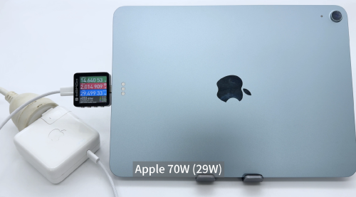
About half the size of an Apple 61W PD charger.

It weighs 120.8g/4.3oz (official data 126g/4.5oz), which is much lighter than the Apple 61W PD charger (208.2g/7.3oz).

It remains stable when plugged into the wall socket.
II Review
1. Charging protocols test

Using ChargerLAB Power-Z FL001S USB power tester, we know that it supports USB PD, QC 2.0, and QC 3.0 protocol.
2 PDO information

PDO information (using normal 3A USB-C to USB-C cable) reveals the USB-C port supports USB PD 3.0 with output in 5V/3A, 9V/3A, 12V/3A, 15V/3A, and 20V/3A.

PDO information (using E-marked 5A USB-C to USB-C cable) reveals the USB-C port supports USB PD 3.0 with output in 5V/3A, 9V/3A, 12V/3A, 15V/3A, and 20V/3.25A.
3. Compatibility test

Charging the iPhone XS Max, we are getting 9.2V 1.84A 16.95W, under PD protocol.

Charging the iPad Air2 which doesn't support USB PD, we are getting 5.2V 2.62A 13.67W, under Apple 2.4A protocol.

Charging the iPad Pro 10.5-inch, we are getting 15.23V 1.85A 28.27W, under PD protocol.

Charging the iPad Pro 11-inch, we are getting 15.23V 2.11A 32.28W, under PD protocol.

Charging the MacBook Pro 13.3-inch, we are getting 20.31V 2.7A 54.86W, under PD protocol.

Charging the Dell XPS13, we got a pop-up window from Dell Power Manager saying it can't recognize the USB-C device. But the charging is fine at 20.34V 2.21A 45.1W, under PD protocol.
III Teardown

We first tried rubber hammer to crack it open, but the sonic soldering was so firm that we finally have to cut it open.

Our sneak peak of the PCBA inside the charger.

What comes into view is the USB-C port which is fixed onto a small daughter board. It is installed vertically on the main control PCBA, next to is are two solid capacitors for output filtering. The transformer wrapped by yellow tape is behind the capacitors.

Remove the case and we have the PCBA. Its four faces are all wrapped with heat sinks which are divided into two pieces. One of the heat sinks wraps three faces, works as heat dissipation for components including the transformer.

Another heat sink is used to dissipate heat for the patch components on the PCB, and several tapes are applied to the heat sink for insulation.

Prepare to remove the heat sink that covers the main control PCB. There is a solder joint on the lower right button of the heat sink, and the rest is fixed using thermal paste.

Remove the heat sink, we find a plastic insulation plate on the inside, and insulation tape is used near the primary input side to ensure insulation reliability. Two pink thermal pads are used between the heat sink and the PCB. One for the primary switch and the other for the secondary synchronous rectifier, which are the two heat-generating power devices.

After cleaning the thermal adhesive, we have a clear view of the PCB board which uses a black oil process. We can see the “POWERLAND” logo between the primary and secondary.
Next, allow me to introduce the main SMD components on the main PCB board:

Starting from the primary side, the rectifier bridge is not seen on the main PCB. So let's begin with the primary controller chip, a PWM controller from Leadtrend, model LD5763GS. It is a green mode PWM IC built-in with brown-in/out functions in an SOP-8 package. It minimizes the component counts, circuit space, and reduces the overall material cost for the power applications. It also features HV start, green-mode power-saving operation, and internal slope compensation, soft-start functions to minimize the power loss and enhance the system performance.

With complete protection in it, as OPP (Over Power Protection), OVP (Over Voltage Protection), fast OSCP (Output Short Circuit Protection) and brown-in/out protection, LD5763GS prevents the circuit from being damaged under abnormal conditions. Furthermore, the LD5763GS features frequency swapping and soft driving function to reduce the noise and improve EMI.

The primary switching tube next to the primary PWM controller is the IPL60R365P7 from Infineon. It belongs to the CoolMOS series, in a ThinPAK 8×8 package.

Detailed specifications of the Infineon IPL60R365P7.

Looking at the secondary side, the synchronous rectifier is also an Infineon MOS, model: BSC098N10NS, 100V 9.8m ohm, Vth 3.8V max.

Detailed specifications of the Infineon BSC098N10NS5.

MPS908 synchronous rectification controller from MPS with letter code IAZEH, Sot23-6, and supports CCM.

Detailed specifications of the MPS MPS908.

The primary and secondary have a wide safe distance, with an optocoupler in the middle. Weltrend WT6636F is used as the USB-C interface controller. It is a protocol chip (TID No. 1080018) certified by the USB-IF USB PD3.0 (PPS), and it is the first time it is seen inside a charger.

AON7544 output switch MOS.The above is the introduction of the main components on the main control PCB board. Now let's move on to disassemble another heat sink.

The heat sink is fixed with three solder joints.

After removing the heat sink, we can see that the area on the inside corresponding to the transformer is affixed with a pink thermal pad. And a plastic insulating plate is used to enhance insulation.

Remove the plastic insulation plate, it can be seen that a large amount of thermal adhesive is used between the components to improve the integrity and strength.

The transformer is made by DVE, and the two solid capacitors at the output with specifications of 25V 680uF and 25V 470uF, respectively.

The two blue Y capacitors are soldered on both sides of the PCB board. Only one horizontally mounted electrolytic capacitor is used in the primary side. The large input capacitor and the transformer account for almost two-thirds of the PCBA.

The electrolytic capacitor is fixed on a daughter board to form a plug-in module. A pink thermal pad is attached to the PCB.

Below the pink thermal pad is the primary rectifier bridge.

Remove the primary electrolytic capacitor and rectifier bridge module.

A capacitor from AiSHi.

A specification of 400V 100uF, which meets the requirements of high power output.

Remove the opposite PCB module with common mode inductor, a Y capacitor and a slow blow fuse on top.

A slow blow fuse, 3.5A 250V.

X safety capacitor at the input side.

Try to remove the PCB board with the fixed USB-C port, only to remove the USB-C socket.

A large amount of thermal adhesive is also used between the transformer and the PCB.

All the components.
IV Conclusion
With clever layout and carefully selected components, engineers at Powerland managed to pull off a powerful and compact solution that doesn't break the bank. It is textbook in design of conventional high wattage PD charger.
Thanks to its all around heat dissipation design, the PA65 doesn't overheat despite its high power density. Pity the prongs are unfoldable.
Pros:
Powerful and compact.
Nice build, good components, and neat layout.
Resonable price.
Cons:
Unfoldable prongs.
Note: ChargerLAB is reader-supported. Our editors independently research, test, and recommend the best products. We may earn commissions on purchases made from links on our site.
Source: chongdiantou

