Introduction
In recent years, the rapid growth of artificial intelligence (AI), cloud computing, and high-density power demands has posed significant challenges to power electronics systems in terms of efficiency, power density, and thermal management. Traditional silicon-based MOSFETs, constrained by material limitations, are encountering performance bottlenecks in high-voltage and high-frequency applications. Gallium Nitride (GaN) technology, with its wide bandgap properties, high electron mobility, and low switching losses, is emerging as the key to overcoming these limitations.
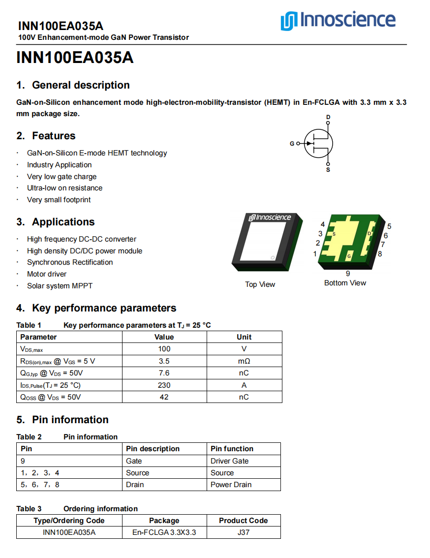
Innosicence has recently introduced the 100V enhancement-mode GaN power device, INN100EA035A, which is the world’s first mass-produced 100V GaN solution. Through innovative double-sided cooling packaging and optimized design, this device redefines the performance boundaries of power systems, providing a new, high-efficiency energy conversion solution for AI servers and 48V infrastructure.
INN100EA035A Overview
The INN100EA035A features a Topside Cooling En-FCLGA package, making it the industry’s first mass-produced P2P silicon MOS 100V GaN product. With an ultra-low on-resistance of 3.5mΩ and double-sided cooling, it offers superior characteristics such as low conduction resistance, low gate charge, low switching loss, and zero reverse recovery charge. These attributes are crucial for high-efficiency AI and 48V power applications. Compared to traditional MOSFET solutions, this device achieves a 20% increase in power density, while reducing system power loss by over 35% compared to the most advanced MOSFETs in the industry.
One of its primary advantages lies in its advanced dual-cooling En-FCLGA package. Traditional single-sided cooling packages have a single heat dissipation path, which can lead to localized hotspots. In contrast, the En-FCLGA package introduces a double-sided heat dissipation architecture, reducing thermal resistance to 0.49°C/W—a 65% improvement in thermal conductivity compared to similar single-sided solutions. This enhancement significantly lowers device junction temperature. When combined with its ultra-low 3.5mΩ on-resistance, steady-state power loss is reduced by over 35% under 48V/25A operating conditions compared to silicon-based MOSFETs.

In AI server 48V DC-DC power architectures, the INN100EA035A utilizes a vertical current path design to minimize PCB parasitic resistance. Compared to conventional MOSFETs, it improves power density by 20%, with system-level efficiency exceeding 98% at full load. This reduces cooling requirements and overall system costs. The dual-sided cooling design also supports flexible integration with multi-layer PCBs and external heat sinks. For example, when paired with a 35×35×15 mm heat sink on a four-layer FR4 board, the junction-to-ambient thermal resistance can be further reduced to 26.22°C/W, meeting the thermal demands of high-power AI GPUs.
Beyond AI server power applications, this device also demonstrates strong competitiveness in fields such as solar MPPT, synchronous rectification, and motor drive applications due to its low-loss and high-frequency characteristics.
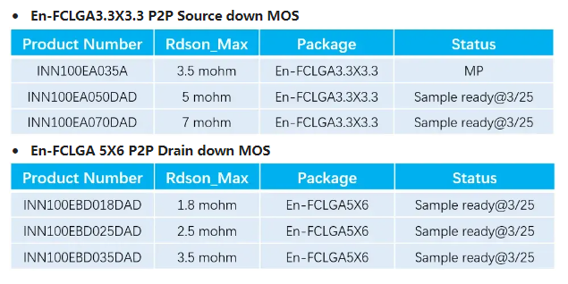
Innosicence has also introduced multiple products based on the En-FCLGA packaging technology, covering an on-resistance range of 1.8-7mΩ. While the INN100EA035A has already entered mass production, other models are currently in engineering validation and are expected to be launched soon. By accelerating the expansion of its GaN product line, Innosicence aims to meet the diversified and customized demands of AI servers, renewable energy inverters, and other power applications. This provides designers with a seamless, cost-effective transition from traditional MOSFETs to GaN solutions.
Summary
The introduction of the INN100EA035A marks a significant breakthrough in GaN power devices, particularly in system integration and thermal management. The En-FCLGA package, featuring a dual-sided cooling architecture and low parasitic parameters, effectively addresses the efficiency and reliability challenges of high-power density scenarios. From a technical perspective, the combination of 3.5mΩ on-resistance, 7nC gate charge, and 42nC output charge gives this device a distinct performance advantage in 48V bus architectures. Compared to existing silicon-based solutions, this GaN device not only increases power density by 20% but also eliminates reverse recovery charge, reducing high-frequency resonance risks and offering superior semiconductor solutions for AI server power supplies, solar MPPT, and motor drives.
With this product, Innosicence further solidifies its technological leadership in the GaN market. The large-scale adoption of double-sided cooling packaging may drive a paradigm shift in power module design from single thermal path optimization to three-dimensional thermal-electrical co-design. As this technology extends to higher voltage levels, GaN devices are expected to achieve wider adoption in electric vehicle powertrains, industrial inverters, and beyond.