Introduction
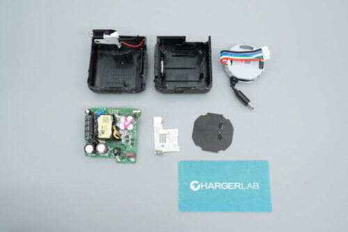
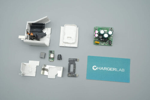
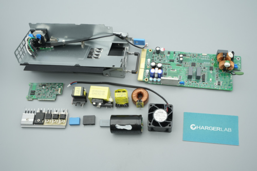
As a member of the third-generation semiconductor family, GaN devices have already demonstrated their reliability and longevity in applications such as fast chargers and other low-power products. The usage of third-generation semiconductors in chargers and power banks allows for increased power density, reduced size, and more ports, making it more consumer-friendly. For high-power applications, such as portable power stations, the use of GaN devices significantly reduces switch losses, enhances conversion efficiency, and lowers heat dissipations and overall costs.
Fans who regularly follow ChargerLAB's teardown articles and videos are aware that GaN has already made its mark in high-power scenarios. However, what most people may not know is that there exists a special day dedicated to Gallium Nitride that we have been leading—GaN Day. In this article, we will delve into its origins and relay the perspectives of various industry experts on the future prospects of the third-generation semiconductor industry, discussing the industry's present and future together.
Origin of GaN Day
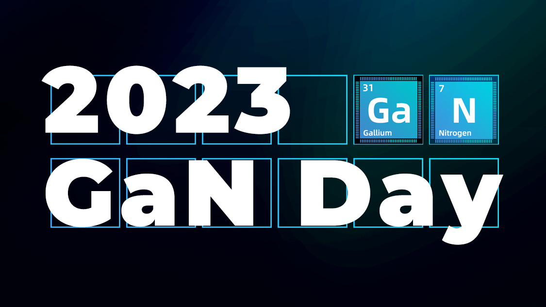
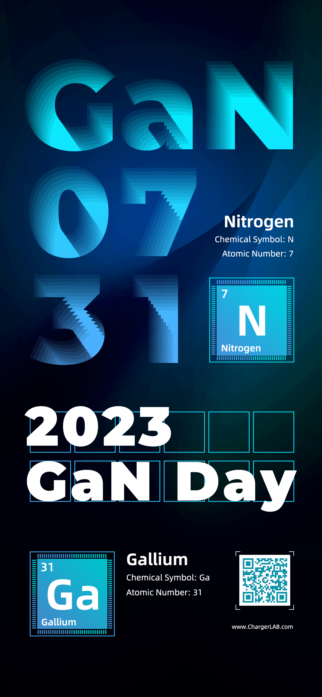
GaN is a compound material composed of nitrogen and gallium. Nitrogen ranks 7th in the periodic table of elements, and gallium ranks 31st. Hence, July 31st was named GaN Day and has gained widespread recognition within the industry. Since ChargerLAB, in collaboration with multiple third-generation semiconductor companies, first proposed GaN Day as a commemorative event in 2020, it has gained significant recognition up to the present time.
Each year, around GaN Day, the third-generation semiconductor industry holds relevant events to celebrate the innovative applications of new GaN technology in various fields. This year is no exception, as we continue the tradition.
Insights from Industry Experts
Innoscience
CEO Jay Son

GaN has become a highly acclaimed material in the realm of third-generation semiconductors. In 2020, it witnessed a groundbreaking application in the fast-charging sector of smartphones, marking a significant milestone for the GaN industry. In 2022, the demand for GaN expanded beyond the vast consumer electronics market. Spurred by new technologies such as AI, communications, autonomous driving, and energy storage, GaN is gaining more and more interest in applications like data centers, automotive electronics, and green energy. The first half of 2023 witnessed an exciting series of events in the GaN industry, such as exciting news of new product launches, industry mergers and acquisitions and a substantial surge in product shipments. It creates a promising future for GaN.
As a leader in the GaN industry, Innoscience has surpassed 270 million units in shipments, and our sales revenue in the first half of 2023 increased by 500% compared to the same period last year. What's more, our product applications have expanded beyond consumer electronics, extending into domains like data centers, automotive electronics, green energy and energy storage. Innoscience stands out among other GaN companies with the cutting-edge 8-inch silicon-based GaN research and manufacturing platform, boasting a comprehensive lineup of high, medium, and low-voltage GaN products. Currently, we can produce 15,000 wafers per month, which gives us a distinct advantage in large-scale manufacturing. Thanks to our integration of design, research and development, production, and sales, we can swiftly adapt and iterate our products to propel terminal applications forward. As the GaN market continues to surge, we would like to collaborate with both upstream and downstream enterprises, leading the way towards a standardized GaN industry chain and expediting the development of the industry ecosystem.
Power Integrations
Doug Bailey - VP Marketing

Power Integrations is finding is that for compact power supplies with a higher spec, GaN is the lowest cost approach. This is because GaN efficiency reduces or eliminates heat sinks and allows the designer to use a simple flyback, which eliminates the extra switches necessary for complex topologies such as LLC or asymmetric half bridge (AHB).
But optimizing the potential of GaN requires new system-level thinking. The old topologies that were invented to compensate for the challenges of using silicon are not required, because GaN is much closer to being an ideal switch. By that I mean that GaN devices switch very, very fast, they have a very low gate capacitance, and very low output capacitance COSS. But that brings with it a different set of design challenges. Power Integrations has found that the best way to work with GaN is to integrate it into a single package with the controller ICs. We have created sub-systems in GaN, such as our InnoSwitch™ flyback power supply ICs, our power factor correction HiperPFS-5™ parts and our LytSwitch-6™ LED drivers. The products that we've built do a beautiful job of addressing notebook adapters, cell phone adapters, small power supplies, LED lighting etc, but there are many applications that we still have to address, so our biggest challenge is completing these system level designs and bringing them to market.
Because GaN approaches the idea switch, my view is that when “GaN can, GaN should”. I see GaN basically taking over at the lower voltages - mains through to 1200 volts; essentially GaN will subsume the entirety of that market up to a certain power level, especially for variable power applications. It's about the technical development of GaN: as the voltage of GaN increases it will replace silicon carbide, and as its current carrying capacity increases, GaN will replace IGBTs.
CorEnergy
Gavin - Founder and General Manager

While another GaN Day is coming, as a veteran in the GaN industry, I am very happy to see that GaN devices and their application solutions are recognized and used by more and more customers. The charging expo held in Shenzhen in the first half of this year, the huge number of participating manufacturers and visiting customers shows how hot the GaN industry is at this moment. In the context of "dual carbon," almost all industries are facing profound challenges of low-carbon transformation, and new semiconductor material technologies will lead the transformation of the energy industry and realize innovation-driven development. GaN devices can bring advantages in performance, size and weight to power modules, making a significant contribution to the sustainable reduction of carbon emissions.
The vision of Corenergy is to shape a greener world with GaN. In the application fields, GaN still has a large growth space in the consumer electronic segment, because more and more consumers are keen to use fast chargers with smaller size, lighter weight and faster speed. This provides a good market opportunity for GaN fast chargers. At the same time, the release of the PD 3.1 fast charging standard is a milestone upgrade for the charger industry. It has broken through the long-standing 100W limit and achieved a double increase to 240W. At the same time, the output voltage has also achieved the maximum coverage of 48V, which can meet the application of consumer, industrial and other multi-field products to further expand the applicable market of GaN fast chargers.
Further, the unification and upgrading of PD standards will help consumers choose chargers that can meet their needs from more product brands and types, and promote further growth in demand. In addition, GaN will experience explosive growth in the segments of energy storage, data centers and new energy in the next 2-3 years. For example, GaN devices can help the development of new electric vehicle charging piles to achieve the goal of a few minutes of charging for a few hundred kilometers of driving, eliminating the mileage anxiety of electric vehicle drivers and boosting the market of electric vehicles.
I believe that in the next few years, GaN will be hotter than the current SiC market. Therefore, Corenergy's R&D, products and applications are also moving from consumer electronics to industrial-grade applications. In terms of competition in the GaN industry, European and American companies still have relatively large advantages in basic technology, innovation, and patent accumulation, while domestic companies have advantages in applications, markets, and manufacturing, and are catching up in technological innovation. In the context of domestic substitution and with the trend of re-globalization, Chinese companies, including Corenergy, have made and will continue to make great progress, making their contribution to a lower-carbon and greener world.
DGCX CAP
Liu Yuanxin - CEO

Gallium Nitride (GaN) technology is the future of charging advancements, spanning mobile phone, laptop chargers, outdoor power banks, smart lighting, and vehicle charging/electricity conversion devices. With its immense market potential and technological growth, GaN technology will prioritize low loss, high stability, and high power density in the charging sector. As GaN technology continues to evolve, it will revolutionize various emerging fields like power transmission, medical equipment, photovoltaic energy storage, electric vehicles, and aviation power, marking a new "energy conversion revolution."
With over 20 years of expertise in ultra-miniature capacitor technology, Chengxi People focuses on capacitor research, production, sales, and service. We strive to provide the world with safe, reliable, energy-efficient, and environmentally friendly capacitor components, aiming to become a leading capacitor brand globally.
GaN Systems
Andy Chuang - VP of Business Development

The development of third-generation semiconductors, led by gallium nitride (GaN) and silicon carbide (SiC), plays a pivotal role in supporting China’s wide-ranging targets for climate mitigation, the so-called “dual carbon” goals and fostering a highly digitalized and electrified society. GaN power semiconductors, in particular, are currently experiencing a tipping point of explosive adoption, expanding their use from fast chargers of consumer devices to data centers, renewable energy systems, industrial motor systems, and electric vehicles, thereby contributing to the optimization of power system efficiency in these application areas.
As a killer application for GaN power semiconductors, the electric vehicle sector has witnessed rapid growth in recent years, achieving record-breaking sales. China has taken a leading position in the development of electric vehicles. Not only have the unit sales surpassed other countries, consumers shifting attitudes toward electric vehicle purchases occurred earlier. The main determinant of electric vehicle purchases is transitioning from subsidies to considerations based on functionality and price. In response to this trend, GaN power semiconductors have become another focal point, after silicon carbide, for research and development in electric vehicle manufacturing. The goal is to leverage the exceptional characteristics of GaN power devices to achieve breakthroughs in efficiency, driving range, and even total bill-of-material costs, with GaN already showing accelerated applications in On-Board Chargers and DC-DC converters.
The widening adoption of GaN across multiple applications for enhanced efficiency, power density, and cost-effectiveness has sustained strong momentum in the power semiconductors sector, even amid economic headwinds. We believe that cross-industry collaborations and talent investments are essential to shorten the learning curve for GaN power semiconductor technology and unlock more application possibilities.
Vergiga
Chairman - Leo.Lee

In recent years, with the joint efforts of the whole industry chain, GaN power devices have rapidly occupied the fast-charge consumer market, basically realizing the market replacement of Si-based devices. From the initial 65W development to today's 18W-300W PD fast charger, GaN power devices have proved to the market its superior performance and brought power density and cost advantages, and its reliability has gradually been recognized by the market.
Driven by the market and the efforts of the industry, the cost of GaN power devices has been gradually reduced to close to that of silicon-based devices, and it is expected to replace silicon-based devices in other consumer markets such as home appliances and adapters. At the same time, based on the gradual improvement in the performance and reliability of GaN power devices and the improvement of market recognition, major manufacturers are actively deploying and promoting the application of GaN devices in the industrial end, such as micro-inverters, data centers, and energy storage and so on. In terms of localization, GaN power devices already have a domestic industry chain from substrate and epitaxy to finished products, and it is expected to achieve corner overtaking in the third generation of semiconductor devices.
Vergiga Semiconductor has always focused on the research and development of power devices and their application technology. With ten years of research, Vergiga Semiconductor has become one of the few advanced semiconductor design companies with a full range of silicon-based low-voltage, medium-voltage and high-voltage full-range power MOSFET / IGBT devices and modules, as well as special semiconductor process design capabilities. semiconductor design company. At the same time, in order to accelerate the process of domestic self-reliance of power devices, Vergiga Semiconductor actively deploys the third-generation semiconductors, and develops a number of SiC MOSFET and GaN HEMT series products.
TI
Product Line Manager for GaN - Abhi Muppiri

The number of companies replacing silicon with GaN is growing rapidly as GaN becomes a key technology to improve power density and increase efficiency in power systems across multiple applications including data centers, telecom power supplies, solar inverters and power delivery applications. From TI’s perspective, the below 3 reasons explain how GaN is changing power management:
While GaN may be perceived as a challenging technology to design with, our company simplifies GaN designs by integrating a gate driver, as well as several protection features, in the chip, enabling designers to get the maximum benefit from the technology by delivering a huge performance benefit and making designing with GaN a lot easier.
GaN has been in development for a number of years and its reliability is established. Our company’s GaN chips have achieved more than 40 million hours of reliability testing, passed automotive qualifications, and has already been adopted in demanding industrial sectors for over 5 years.
Today, GaN is more expensive than silicon in chip-to-chip comparisons, however, its benefits to the overall system cost, improvements in efficiency and power density outweigh the initial investment. For example, an efficiency gain of as little as 0.8%in a 100-megawatt data center using a GaN-based power management system can save $7 million in energy costs over 10 years.
LIHOMICRO
CEO - Sam Chung

With the rapid development of semiconductor devices, The third generation semiconductors have entered the fields of new energy vehicles, photovoltaic inverters, 5G base stations, PD fast charging and so on. SIC devices are mainly used in new energy vehicles and industrial control fields, and Gan devices are mainly used in 5G base stations and power supplies. Compared with the silicon devices, SIC MOS has lower on resistance and fast switching speed at high voltage and high cutrent, which is especially suitable for inverter applications of new energy vehicles. The new round of industrial development brings a huge market prospect for the third generation semiconductor devices.LIHOMICRO SIC devices will improve the technology upgrade and product iteration according to the different needs of customer groups and the use of more and more customers, which is expected to promote the industry development.
TAGOR
VP of Market Development - Tino Pan

When discussing the characteristics of gallium nitride (GaN) materials, we should not limit its applications solely to power products. GaN has numerous outstanding properties, particularly in the wireless communication market where it is highly suitable. Shenzhen Tagoretech Co., Ltd( The following will be referred to as "Taigao").is a semiconductor company specializing in GaN RF front-end chips. With its invention patents in the field of GaN RF, the company has successfully developed a series of high-power GaN RF front-end chips. These innovative chips significantly enhance wireless communication distance and improve image transmission quality. With Taigao GaN design, these chips have higher power density and lower energy consumption. This innovative technology not only improves the overall performance of products but also brings revolutionary breakthroughs to the field of wireless communication. The key technology of Taigao GaN RF devices increases the coverage range in densely populated areas by 4.5 times. Additionally, in line-of-sight limited environments, the transmission distance is doubled, and the transmission rate is increased by 2-4 times. At the same time, power loss is reduced by more than 10 times while maintaining the same communication range and throughput.
Summary of ChargerLAB
The widespread application of third-generation semiconductors has revolutionized the traditional power conversion methods. By reducing switching losses and increasing the switching frequency of power supplies, it achieves two significant benefits. On one hand, it reduces the size of power supplies, and on the other hand, it enhances conversion efficiency, bringing noticeable technological advancements to consumers. Looking ahead, Gallium Nitride (GaN) devices will play a pivotal role in higher-power applications, improving the efficiency of power systems, reducing energy wastage, and promoting the implementation of green and low-carbon principles.
Related Articles:
1. Navitas Celebrates 75,000,000 GaN Power Shipments
2. Innoscience Demonstrates the Ubiquitous Presence of GaN at APEC
3. Navitas Takes GaN Integration to Next Level with GaNSense Control

