At CES2019. Aukey announced the development of three ultra-fast GaN-based wall chargers: a 27-Watt USB-C model (PA-Y19), a 30-Watt USB-C model (PA-Y21) and a 24-Watt charger with two USB outputs (PA-U50). These power supplies are designed using GaNFast™ devices from Navitas Semiconductor. Today we are going to teardown the smallest one of the three, the 27W PA-Y19.
I. Design

Aukey 27W USB PD GaNFast comes with an industrial card box, no fancy stuff.

GO GREEN WITH AUKEY.

A warranty card and a user manual.

The charger is a square box in pure white. Under the AUKEY logo is a green USB-C port with PD lettering.

Foldable prongs, US standard.

Detailed product specifications on the side of the charger. Model PA-Y19, input support 100-240V~ 0.65A 50/60Hz, output supports USB PD fast charging, output: 5V/3A, 9V/3A, 12V/2.25A, 15V/1.8A, 20V/1.35A, maximum 27W. The product has passed the VI (6) energy efficiency level, and has CE and RoHS certification.

In comparison, the AUKEY 27W PD charger is about half the size of the Apple 30W charger, one and a half size of the Apple 5W charger. So the AUKEY has a very high power density.

With ChargerLAB Power-Z KT001 USB Power Monitor, we know that the AUKEY 27W PD charger supports USB PD 3.0 protocol with 5V/3A, 9V/3A, 12V/2.25A, 15V/1.8A, 20V/1.35A 27W max output.

It also supports Apple and USB DCP charging protocol.

Use the AUKEY 27W PD charger to charge the iPhone XS, our ChargerLAB POWER-Z KM001C reads 9.03V 2.01A 18.2W, under PD protocol.

Our Mate 20 Pro (UD) is getting 9.02V 1.8A 16.28W, under PD protocol.

Our Mi8 is getting 9.03V 1.83A 16.56W, under PD protocol.

Charging the iPad Air 3 at 15.02V 1.73A 26.05W, under PD protocol.

Charging the MacBook Pro at 19.7V 1.29A 25.54W, under PD protocol.
II Teardown

The charger can be opened from its plug area.

The internal consists of multiple PCBs.

An insulating frame is used between the PCBs to provide insulation and support for enhanced strength. The lower PCB board is the primary side, and the input end is soldered with two metal domes for connecting with the pins.

The gap between the parts inside the PCB is filled with the thermal paste.

From the output side, the inside of the PCB is almost filled with glue. The USB-C port is soldered and fixed to the secondary PCB through a small PCB. The vertical PCB on the right is connected to the primary side and the secondary side, with a primary rectifier bridge, optocouplers, X capacitors, and other components.

On the outside of the side PCB board is a rectifier bridge and an optocoupler.

2A rectifier bridge.

CT1018 optocoupler for output voltage feedback and protection.

Taking a look at the outside of the primary PCB. The largest component is the GaN GaNFast power IC from Navitas, and on the upper right corner is the main control chip.

The NV6252 is a high-performance, easy-to-use, world's first half-bridge GaNFast power IC, optimized for high frequency, soft-switching topologies. The feature-rich, monolithically-integrated GaNFast power IC with simple logic inputs, harnesses two high performance eMode GaN FETs (600 mΩ high-side, 300 mΩ low-side) to create the fastest, smallest, most efficient powertrain in the world. GaNFast power ICs extend the capabilities of traditional topologies such as flyback, half-bridge, buck/boost, resonant, etc. to MHz+ and enable the commercial introduction of breakthrough designs. We have seen the adoption of GaNFast ICs on products like the Anker PowerCore Fusion PD and RAVPower 45W GaN PD.

Detailed specification of the Navitas NV6252 GaNFast Power IC.

UCC28780 from TI is a high-frequency active-clamp flyback controller that enables high-density AC-to-DC power supplies with a variable switching frequency of up to 1 MHz. User programmable advanced control law features allow performance to be optimized for both Silicon (Si) and Gallium Nitride (GaN) power FETs.

Detailed specification of the TI UCC28780.

The three chips on the outside of the secondary PCB are synchronous rectification controller, synchronous rectification MOS tube and USB PD protocol chip.

MPS MP6908A synchronous rectification controller, a fast turn-off intelligent rectifier that supports 600kHz switching frequency.
Detailed specification of the MPS MP6908A.

AO AONS62922 output synchronous rectification MOS tube, NMOS, withstand voltage 120V, low resistance, optimized for synchronous rectification.

Detailed specification of the AO AONS62922.

The Weltrend WT6615F is used for PD protocol and feedback to regulate the output voltage.

The WT6615F is a highly integrated USB Power Delivery (PD) controller that supports USB PD 3.0 Programmable Power Supply (PPS) specification and Qualcomm Quick Charge 4 or Quick Charge 4+ technologies designed for USB Type-C Downstream Facing Port (Source) charging applications such as power adapters, wall chargers, car chargers, power strip, power banks, and etc.
Next, we take apart the PCBs and check out more internal details.

0.1μF X capacitor and input common mode inductor to suppress interference.

Blue Y capacitor across the primary side and the secondary side.

Two high-voltage electrolytic capacitors with specifications of 400V 22μF. There is a magnetic loop inductor between the two capacitors. The red patch component is an input fuse.

A copper foil is grounded on the transformer core to reduce interference.

The secondary multilayer insulation wire of the transformer is directly soldered to the small output PCB.

Two output 180μF 25V solid capacitors are parallelled for filtering, and the output port PCB is soldered to the lower board.

1R0 output filter inductor.

Output current sense resistor and VBUS switch tube to provide overcurrent short circuit protection for output.

A Y capacitor across the two PCBs.

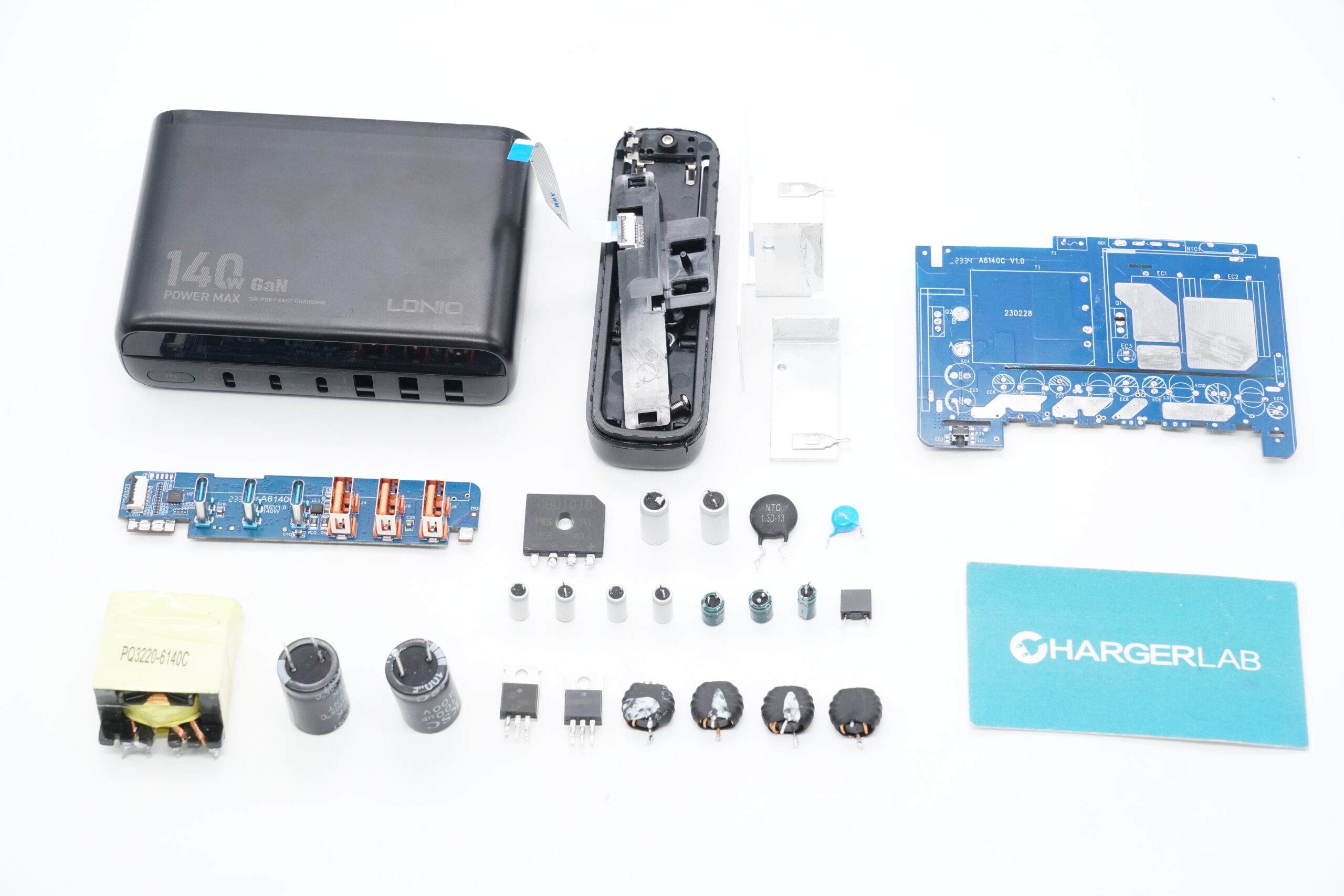
All the components.
III ChargerLAB conclusion
By comparing the size of the AUKEY 27W USB PD GaNFast charger with conventional USB PD chargers, we can clearly see the advantages of the former in terms of compactness, which has twice the power density of conventional chargers. The AUKEY 27W USB PD GaNFast charger is not only compact, but also has foldable prongs for better portability. It has a full range of USB PD output voltage and is compatible with both phones and laptops.
In our teardown, we found that this charger introduced the GaNFast technology by Navitas, with the world's first integrated drive half-bridge GaN IC - the NV6252 built in. The high integration of the chip omits the peripheral driver circuit, and the high efficiency eliminates the heat sink, which are the main reasons why this charger can be so small yet powerful. In addition, this charger uses multiple PCB design, which maximizes the space usage inside and further shrinks the size of the charger.


