We did a quick hands-on review of the Anker PowerPort Atom PD 4 charger a few weeks ago. It supports a maximum of 100W PD charging and has 2A2C four ports. But no ChargerLAB review is complete without a teardown review. So, let's take an inside look of this brand new desktop charger.
I Unboxing

Classic ANKER package design featuring a clean white box with blue accents.

Specifications on the back. Model: A2041. Weight (including AC cable): 447g (15.77oz). Size: 110*86*34mm (4.33*3.39*1.34in). Made in China. Input: 100-240V~ 2A 50-60Hz. Max output: 100W. USB-C output: 5V/3A、9V/3A、15V/3A、20V/5A. USB-A output: 5V/2.4A (max).

The power bank lays inside the blue paper tray.

Package contents: charger, figure-8 power cord, Velcro cable tie, foam tape, user manual, warranty card, qualification certificate, and list of hazardous substances in electronic products.

A foam tape to position the charger on the desktop or on the wall.

A high quality figure-8 power cord.

The ANKER PowerPort Atom PD 4 100W charger is made of flame-retardant plastic with glossy piano paint process, offering a delicate touch.

Rounded corners bring nice hand-feel.

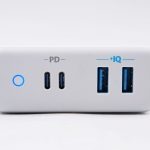
The output panel is light gray with a matte finish. It has 2 USB-C ports, 2 USB-A ports, commonly known as 2A2C configuration. They are all in signature Anker blue color with protocol lettering on the top. There is a ring-shaped power indicator on the left, which emits blue light when the power is turned on.

Figure-8 power input port.

Non-slip rubber pads.

Specifications. Input: 100-240V~ 2A 50-60Hz. USB-C output: 5V/3A、9V/3A、15V/3A、20V/5A. USB-A output: 5V/2.4A (max). Max output: 100W. Designed by ANKER. Made in China.

Compared to the Apple 87W PD charger.

Compared to a 1 Yuan RMB coin.

It weighs 373.1g (13.2oz).
II Review
1. Charging protocols test

With ChargerLAB Power-Z KT001 USB Power Monitor, we know that its USB-C port supports USB PD protocol and USB-DCP-5V-1.5A.

The two USB-C ports are the same.

With ChargerLAB Power-Z KT001 USB Power Monitor, we know that its USB-A port supports Apple 2.4A charging protocol.

The two USB-A ports are the same.
2. PDO reading

PDO information reveals its USB-C port is capable of PD2.0 quick charging output in 5V/3A, 9V/3A, 15V/3A, and 20V/5A.

The two USB-C ports have the same PDO reading.
III Teardown

Pry open the gray output port cover which uses clips to snap into the body. A design that enables non-destructive opening.

The upper and lower casings are ultrasonically welded and can be opened by force.

There are two self-tapping screws on the side of the PCBA output end that are fixed to the bottom case.

At the other end of the PCBA, a large amount of white glue is filled between the gaps of the outer casing to fix and conduct heat.

Open the case, we can see the front of the PCBA is covered by a large heat sink, and there are two shock absorbing sponges on the heat sink.

After removing the two fixing screws and cleaning up the glue, we can see there is also a large heat sink covering the primary circuit on the back of the PCBA.

Removing the large heat sink on the front of the PCBA, there is also a small heat sink on the secondary part, and there is a thermal pad on the transformer.

Under the small heat sink are two small PCBAs connected using a thermal pad.

Another small PCBA and transformer, PFC inductor, and rectifier bridge stack have thermal pads to make close contact with the main heat sink.

There are three heat sinks fixed by screws on the three primary switching tubes.

The silicone thermal conductive strip on the other secondary output plate which contacts with the main heat sink.

Remove the secondary small heat sink to reveal two output PCBAs, there is a large amount of white glue between the gaps.

Remove the silicone thermal conductive strip and clean up the white glue so we can have a clear view of the PCBA. The upper part has a plurality of output leads is the switching transformer BCK-10-007T, and the lower part is the BCK-10-010T PFC inductor.

The back of the PCBA after removing the heat sink. The left side is the secondary low-voltage output part, the right side is the primary high-voltage part, the isolation area is wide enough with hollow-out slots and an insulation sheet to strengthen the isolation. The PFC inductor and the switch transformer part have heat dissipation holes.

PCBA primary high voltage part, the main components are two ICs and a feedback optocoupler.

Three white LLC resonant NPO capacitors in parallel connection, which are generally used in higher-end wireless chargers. They have excellent value stability under temperature variations, suitable for high frequency applications with low loss and better energy efficiency. Applications here require a withstand voltage of up to 630V.

TEA19162 PFC controller from NXP for boosting the rectified and filtered voltage.

Detailed specifications of the NXP TEA19162.

TEA19161T the LLC controller, teams with the TEA19162 to form a switching power supply with APFC to improve the power conversion efficiency.

Detailed specifications of the NXP TEA19161T.

TCLT1007, wide pitch high isolation patch optocoupler.

NXP TEA1995 synchronous rectification controller on the secondary side.

Detailed specifications of the NXP TEA1995.
NXP's GreenChip power solution, the new TEA1916+TEA1995 platform offers very high efficiency over the entire load range, especially at light loads of 10-30% -- easily meeting energy efficiency regulations including Energy Star v6, CoC tier 2, 80+ platinum and EuP Iot6. The TEA1916 additionally features low no-load power below 75mW, meeting and exceeding requirements of Energy STAR, DoE, CoC tier 2, etc. The LLC resonant topology also makes it easier to meet Common Mode Noise requirements and 200% peak power requirements when compared to a flyback topology.

Reference circuit diagram of the TEA19161+TEA19162+TEA1995T solution.

Two Infineon synchronous rectifier MOS tube BSC076N06NS3 G, the parameters are 60V, 50A, 7.6mΩ.

Detailed specifications of the Infineon BSC076N06NS3 G.

Two Infineon MOS tubes BSZ086N03NS3 G, for USB-C1 output VBUS switch, parameters are 30V, 40A, 8.6mΩ.

Two Infineon MOS tubes BSZ086N03NS3 G, for USB-C2 output VBUS switch, parameters are 30V, 40A, 8.6mΩ.

Infineon MOS tube BSZ086N03NS3 G, teams with R005 current-sense resistor and other circuits as the USB-A2 output VBUS overcurrent protection switch.

Detailed specifications of the Infineon BSZ086N03NS3 G.

The 6-pin IC with SEG lettering is TI's INA199B2DCKR current detection chip for overcurrent protection of the USB-C1 output port.

Detailed specifications of the TI INA199B2DCKR.

The USB-C2 output port also uses a TI INA199B2DCKR current-sensing chip.

Detailed specifications of the TI INA199B2DCKR.

The chip with 1101 lettering is the TCP1101 current-limiting chip from Chengyi Semiconductors. It supports a custom current limit point and has a built-in 16mΩ ultra-low on-resistance MOS tube in an ultra-small SOT23-6L package.

Detailed specifications of the Chengyi TCP1101.

The chip with CYPD4225 lettering is the CCG4 USB PD controller IC from Cypress. The SOT23 packaged chip on the right side with V3RD lettering is a voltage regulator from Nanjing Micro One Electronics, which supplies power for CCG4.

CCG4 is Cypress’s newest USB Type-C port controller with Power Delivery. CCG4 provides a two-port USB-C solution ideal for desktops, notebooks and systems like power banks, monitors and docks. It is also used in Huawei P30 Wireless Charging Protective Case.

Regulator tube from Nanjing Micro One Electronics in SOT23 package and V1R1 lettering.

Two intelligent identification chips for USB-A port, the CellWise CW3002G. As seen on the ANKER PowerCore 10000 PD Power Bank (A1235).
Now, let's look at the details on the front of the PCBA:

Top view of the secondary section. There are two USB-C output port boards, one LED power indicator board, three step-down boards, two USB-A sockets, and three common mode inductors. Each of the three step-down small plates has a large inductive coil with multi-strand winding, which is insulated by a double-layer heat-shrinkable tube. There are two horizontally mounted, solid capacitors wrapped by heat shrink tubing between the two buck boards.

The two solid capacitors wrapped by heat-shrink tubing are 100μF, 35V, and are used for input filtering for the voltage conversion boards.

An electrolytic capacitor and three solid capacitors with a withstand voltage of 35V, two 470μF and one 100μF, are used for input filtering of the two USB-C input circuits.

An electrolytic capacitor from Acon, 1000μF 16V.

The LED power indicator board and two USB-C output boards are soldered vertically to the main PCBA. Black foam is placed around the LED to avoid light leakage.

The two USB-C output boards are the same.

There are two MOS and diode components on the back of each USB-C output board. There are no components on the back of the LED power indicator board.

The VBUS switch MOS on the back of the output port board is the AON2408 from AOS, the parameters are 20V, 8A.

Detailed specifications of the AOS AON2408.

Remove the rectifier bridge stack, there are three primary switching tubes, three step-down small plates, and a horizontally mounted solid capacitor.

Three Infineon IPA60R120P7 MOS tubes and a 15A 1000V rectifier bridge stack. The two MOSs with a slightly larger heat sink are the LLC main switch tubes, and the smaller one is the APFC boost tube which has a withstand voltage of 650V and a conduction resistance of 120mΩ, effectively reduces the temperature rise and improves the efficiency and power density.

Detailed specifications of the Infineon IPA60R120P7.

Remove the three MOS transistors and the primary PCBA portion of the rectifier bridge stack, we can see the PFC boost diode on the left side of the two primary capacitors.

Multiple CX capacitors, common mode inductors, and differential mode inductors form a complete EMI filter network.

In order to improve space utilization, the yellow CX capacitor is mounted using a three-dimensional installation, and a common mode inductor is hidden underneath.

Time-delay fuse, 5A 250V in reddish brown color.

Primary filter electrolytic capacitor, 33μF, 450V, from Acon.

Two 33μF 450V high voltage electrolytic capacitors are connected in parallel.

Acon electrolytic capacitor, 22μF, 50V.

Acon electrolytic capacitor, 22μF, 50V.

Acon electrolytic capacitor, 47μF, 50V. Three small-capacity electrolytic capacitors are used here for powering two primary power ICs.

The secondary part after removing some of the components.

Infineon MOS tube BSZ086N03NS3 G, teams with R005 current-sense resistor and current detection chip INA199B2DCKR to constitute a USB-A output overcurrent protection switch.

The 8 lead wires of the switching transformer are covered with a Teflon sleeve.

Another Chengyi Semiconductors TCP1101 current-limiting chip.

Another TI INA199B2DCKR current-sensing chip.

A layer of copper foil traces can be seen in the middle of the PCB.

Three boost boards, the one on the left is used for two USB-A ports, and the two USB-C interface small boards on the right are exactly the same, which are used for two USB-C ports.

The back of the three buck boards are roughly the same, the chips are exactly the same, and the individual RC components are slightly different.

Two different boards. The left one is for the USB-A port while the right one is for the USB-C port.

Board for the USB-A port.

Board for the USB-C port. Two BSC0702LS FETs from Infinoen, 60V/84A, 100°C/2.7mΩ, used as external synchronous rectifier switches for buck chips.

Southchip SC8001 synchronous buck controller chip.

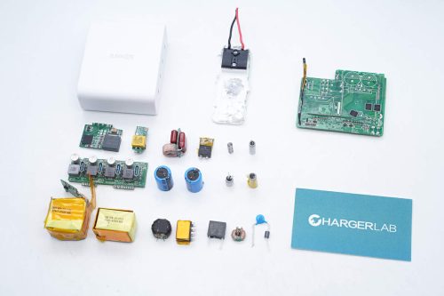
All the components.
IV Conclusion
The Anker PowerPort Atom PD 4 100W offers great versatility and ample power by providing 2 USB-C ports and 2 USB-A ports to cover a wide range of charging needs for devices including phones, tablets and laptops. Its minimalistic design blends perfectly into almost every desktop set-ups.
It can be seen from out in-depth teardown that this power bank features NXP's GreenChip power solution, the new TEA1916+TEA1995 platform which offers low static loss, low voltage ripple, high transient response and high efficiency. The whole system adopts high quality components such as Infineon Power MOS and Acon capacitors.
The charger adopts a secondary buck design. Two USB-A ports share one buck module, while the two USB-C ports each equipped with one buck module. The three DC-DC buck modules all adopt the Southchip SC8001 synchronous buck controller IC. In terms of protocols, the two USB-C ports use Cypress dual-port USB Type-C PD controller EZ-PD CCG4, and the two USB-A ports all implement CellWise CW3002G for 5V/2.4A protocol.
As a result, the Anker PowerPort Atom PD 4 100W is capable of charging phones, tablets, as well as laptops with high energy efficiency and great compatibility.
Pros:
USB-C and USB-A ports covering all charging needs.
USB-C PD with 100W max charging power.
Minimalistic design and high quality components.
Cons:
Expensive (100 USD).
Source: chongdiantou

