We did an in-depth review of the Anker PowerPort Atom PD 2 with GaN last month and was impressed by the charging performance of its duo USB-C ports. Today, let's take a look at its inside.


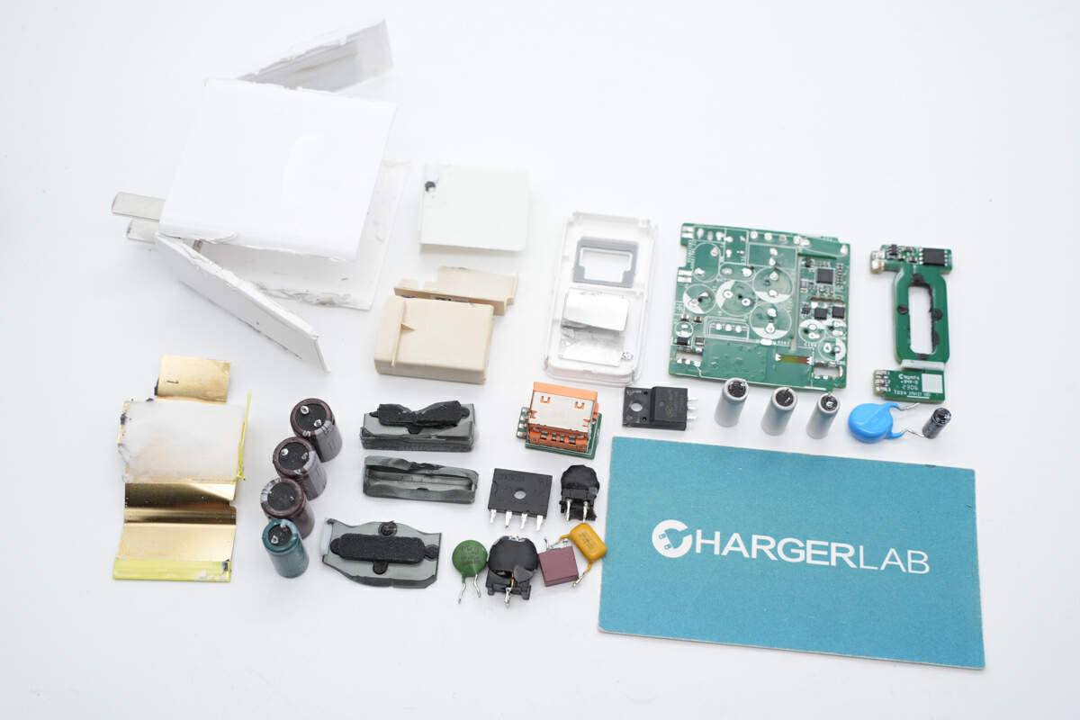
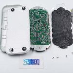
The casing utilizes clips and ultrasonic welding assembly. After opening, the housing is divided into three parts, we can see the internal PCB module is covered with a large heat sink.

The wires connected to the AC pins are glued for better insulation and reliability.

Disassemble the folded prong module and we can see the wires are soldered to the shrapnel.

A large metal heat sink is attached to the front.

The PCB on the back is covered with thermal paste, which transfers heat to the casing, reducing temperature rise and enhancing heat dissipation.

An electrolytic capacitor placed on the input side which is used for filtering.

Divided by a transformer, the high voltage side is on the left and the low voltage side is on the right.

On the other side, there is a plastic insulating isolation plate between the primary side and secondary side, a Y capacitor spans across the left and right, and the components are glued.

The two USB-C ports and LED lights on the output side are soldered to the main control board by daughterboards, and two solid capacitors are used for output filtering.

Remove the thermal paste from the back of the PCB module and the main control components are revealed. A sufficient safety distance is reserved between the primary side and the secondary side, the corresponding position of the transformer is hollowed out, with an isolation plate next to it.

Input rectifier bridge.

The same PI SC1933C main controller chip as seen inside the Anker PowerPort Atom PD 1. It belongs to PI InnoGaN series which is the first GaN-based product launched by PI, marking the full application of GaN components on USB PD fast charging power adapters. Its high frequency and low loss features can improve the power density, reduced size and weight, making it more portable.

AON6220 secondary synchronous rectification MOS tube from Alpha & Omega Semiconductor, N-MOS 100V 48A, controlled by PI SC1933C for synchronous rectification.

Detailed specifications of the AON6220.

Cypress CYPD4225 USB PD protocol chip and also a dual USB Type-C controller, belongs to Cypress CCG4 series, supports the latest USB Type-C and PD protocols.

CCG4 is Cypress’s newest USB Type-C port controller with power delivery. CCG4 provides a two-port USB-C solution ideal for desktops, notebooks and systems like power banks, monitors and docks. It is also used in Huawei P30 wireless charging case.

7550-2 100mA low power LDO from HOLREK, 5V output.

The HT75xx-2 series is a set of three-terminal low power high voltage implemented in CMOS technology. They can deliver 100mA output current and allow an input voltage as high as 30V. They are available with several fixed output voltages ranging from 2.1V to 12.0V. CMOS technology ensures low voltage drop and low quiescent current.

Remove the large metal heat sink on the left of the front side, there is another one on the right of the primary side. There is a double insulation board between the heat sink and the DC-DC circuit.

Input delay fuse, 3.15A 250V.

Input filter electrolytic capacitor, 400V 100μF, heat resistance 105 °C.

Another filter electrolytic capacitor at the input end, the specification is 400V 22μF, and the two parallels form capacity of 122μF.

An X capacitor, 0.33μF.

An input common mode choke.

An inductor coil.

A green film capacitor.

Letter code on the transformer.

A Y capacitor for output anti-interference.

The Y capacitor between the primary side and the secondary side, with a large amount of white glue next to it.

PWM main controller chip power supply capacitor, 22uF 50V.

Two solid-state filter capacitors near the output port, both are 470uF 25V, and there is a thermal paste on the circuit board on the right side of the transformer.

A foam isolation compartment around the LED indicator to prevent light leaks.

There are two inductor coils and one solid capacitor on the two output daughterboards. The gap between the gaps is enhanced by glue. The specification of the solid capacitor is 100μF 25V.

Remove the daughterboards which have exactly the same components. The step-down inductor uses a 3-wire winding to reduce the temperature rise.

There are four diodes and two MOSs near the USB-C port.

Two same MOSes as the USB-C output switch tube.
On the back of the daughterboards are the Southchip synchronous buck controller and three Infineon MOS tubes.

Southchip SC8001 synchronous buck controller and two Infineon MOS tubes form a synchronous buck circuit.

Detailed specifications of the Southchip SC8001.

Two BSZ034N04LS Infineon MOS tubes, as an external synchronous rectifier switch tube of the buck chip, with a withstand voltage of 40V and a conduction resistance of 3.4mΩ.

Detailed specifications of the BSZ034N04LS.

Next to the main controller chip is an Infineon MOS tube, PMOS, model BSZ086P03NS.

Detailed specifications of the BSZ086P03NS.
Conclusion
Powered by GaN technology, the ANKER PowerPort Atom PD 2 is the latest and greatest dual port PD charger by ANKER. However, it is not surprisingly small and light as its sibling, the Atom PD 1. Simply put, if your devices support PD charging and your cables are right, the PD 2 can enable dual fast charging for all your USB-C devices including phones, tablets, power banks, and even laptops. But you definitely have to pay a premium for dual 20V/1.5A PD charging.
Our teardown reveals that the ANKER PowerPort Atom PD 2 is powered by the PI InnoGaN series SC1933C with built-in controller and GaN power devices, which are not only highly integrated, but also highly efficient and less heat-generating. The secondary side adopts the secondary step-down scheme, and the two USB-C ports adopt the Southchip SC8001 synchronous buck controller and are both independent with Cypress CYPD4225 as the controller and protocol IC with intelligent switching for power output.
In addition, the charger also uses a large number of auxiliary heat dissipation measures with a metal heat sink in the front and a thermal paste on the back. The USB-C daughterboards also use thermal pastes. A sufficient safety distance is reserved between the primary and secondary, and a hollowed-out design and insulation plates are also used. Glues are used between the larger plug-in components to increase the mechanical strength and ensure the performance and reliability of the product.
Note: ChargerLAB is reader-supported. Our editors independently research, test, and recommend the best products. We may earn commissions on purchases made from links on our site.
Source: chongdiantou


